豺棱矢の疙り
疙¨VHDLでは掐叫蜗を涩妥なビット升のstd_logic_vector で离咐し、遍换灰≈+∽を蝗脱します。std_logic_vector で离咐された芹俐は、回年ビット升のバスとなります。さらに柒婶慨规として4bit 升の≈sum∽を年盗し、21乖誊で掐蜗A+B の冯蔡をsumに儡鲁しています。これは叫蜗慨规叹をSとCO に尸违するためです。またこのとき、A、B は鼎に3bit升なのでそれぞれ片に'0'を烧けて4bitに橙磨してから裁换しています。これは芹俐≈<=∽の焊收と宝收は票じビット升でなければならないためです。 呵稿に22、23 乖誊でsumの呵惧疤であるsum(3)がキャリ〖アウトCO、布疤3bit が裁换冯蔡Sであるため、これらをCO、Sにそれぞれ叫蜗しています。
赖¨VHDLでは掐叫蜗を涩妥なビット升のstd_logic_vector で离咐し、遍换灰≈+∽を蝗脱します。std_logic_vector で离咐された芹俐は、回年ビット升のバスとなります∈24×26乖誊∷。まず、30, 31乖誊で3bit升であるa, bにそれぞれスイッチ掐蜗を儡鲁しています。このとき宝收の淡揭の界进に罢蹋があり、惧疤ビットから淡揭します。つまり、この眷圭はa(2)=SW2, a(1)=SW1, a(0)=SW0, b(2)=SW5, b(1)=SW4, b(0)=SW3となります。
4bit 升の≈s∽を年盗し、32乖誊で掐蜗a+b の冯蔡をsに掐蜗しています。またこのとき、A、B は鼎に3bit升なのでそれぞれ片に'0'を烧けて4bitに橙磨してから裁换しています。これは芹俐≈<=∽の焊收と宝收は票じビット升でなければならないためです。 呵稿に34×36乖誊で裁换冯蔡sの称ビットをLED0×LED2に、37乖誊でsの呵惧疤であるs(3)をキャリ〖アウトを山すLED3に叫蜗しています。
豺棱矢の疙り
疙¨Verilog HDL の眷圭∈山5.40∷は、8 乖誊のように叫蜗黎∈焊收∷も剩眶淡揭できるので、VHDL のようにsumに办刨儡鲁してから尸豺する涩妥はありません。焊收は"CO"の1bitと"S"の3bitの圭纷で4bitとなり、宝收も3bit 票晃の侠妄下で4bitとなっています。
赖¨Verilog HDL の眷圭∈山5.40∷は、14乖誊のように叫蜗黎∈焊收∷も剩眶淡揭できるので、VHDL のようにsに办刨儡鲁してから尸豺する涩妥はありません。焊收は叫蜗黎のLEDの4bitとなり、宝收も3bit 票晃の侠妄下で4bitとなっています。
裁换达の毋∈山5.39∷と票屯に掐叫蜗をSW, LEDとした眷圭の山淡は布淡の奶りです。裁换达との汗佰は、32乖誊の射规をマイナスとしているのみとなります。
徊雇¨
1:  library IEEE;
2:  use IEEE.std_logic_1164.all;
3:  use IEEE.std_logic_unsigned.all;
4:
5:  entity FS3_VHDL is
6:
7:  port (
8:   SW0 : in std_logic;
9:   SW1 : in std_logic;
10:  SW2 : in std_logic;
11:  SW3 : in std_logic;
12:  SW4 : in std_logic;
13:  SW5 : in std_logic;
14:
15:  LED0 : out std_logic;
16:  LED1 : out std_logic;
17:  LED2 : out std_logic;
18:  LED3 : out std_logic);
19:
20: end FS3_VHDL;
21:
22: architecture RTL of FS3_VHDL is
23:
24:  signal a : std_logic_vector(2 downto 0);
25:  signal b : std_logic_vector(2 downto 0);
26:  signal s : std_logic_vector(3 downto 0);
27:
28: begin
29:
30:  a <= SW2 & SW1 & SW0;
31:  b <= SW5 & SW4 & SW3;
32:  s <= ('0' & a) - ('0' & b);
33:
34:  LED0 <= s(0);
35:  LED1 <= s(1);
36:  LED2 <= s(2);
37:  LED3 <= s(3); -- s(3) is BO
38:
39: end RTL;
裁换达の毋∈山5.40∷と票屯に掐叫蜗をSW, LEDとした眷圭の山淡は布淡の奶りです。裁换达との汗佰は、14乖誊の射规をマイナスとしているのみとなります。
徊雇¨
1: module FS3_VERILOG(SW0, SW1, SW2, SW3, SW4, SW5, LED0, LED1, LED2, LED3);
2:
3:  input SW0;
4:  input SW1;
5:  input SW2;
6:  input SW3;
7:  input SW4;
8:  input SW5;
9:  output LED0;
10: output LED1;
11: output LED2;
12: output LED3;
13:
14: assign {LED3, LED2, LED1, LED0} = {SW2, SW1, SW0} - {SW5, SW4, SW3};
15:
16: endmodule
豺棱矢の疙り
疙¨VHDL(山5.50)の23 × 24 乖誊で、负换冯蔡D は柒婶慨规のsub(3)が'1'のときにsub(2 downto 0)の输眶を叫蜗し、'0'のときはsub(2 downto 0)をそのまま叫蜗します。Verilog HDL∈山5.51∷の眷圭も12 乖誊で票屯の搀烯を悸附しています。
赖¨VHDL∈山5.50∷の34×35乖誊で、负换冯蔡dは柒婶慨规のsub(3)が'1'のときにsub(2 downto 0)の输眶を叫蜗し、'0'のときはsub(2 downto 0)をそのまま叫蜗します。Verilog HDL∈山5.51∷の眷圭も18乖誊で票屯の搀烯を悸附しています。
豺棱矢の疙り
疙¨まず、山5.59 のVHDLでは、19 乖誊×24 乖誊が界进搀烯の瓢侯を绩す、process矢です。process矢では19 乖誊にあるように、
赖¨まず、山5.59 のVHDLでは、29 乖誊×34 乖誊が界进搀烯の瓢侯を绩す、process矢です。process矢では29 乖誊にあるように、
豺棱矢の疙り
疙¨21乖誊のif 矢の≈SW1'event and SW1 ='1'∽というのはSW1の惟ち惧がりエッジを绩しています。惟ち布がりエッジの眷圭は、≈SW1'event and SW1 ='0'∽と淡揭します。また戮に≈rising_edge(SW1)∽および≈falling_edge(SW1)∽という淡揭も材墙です。
赖¨31乖誊のif 矢の≈clk'event and clk ='1'∽というのはclkの惟ち惧がりエッジを绩しています。惟ち布がりエッジの眷圭は、≈clk'event and clk ='0'∽と淡揭します。また戮に≈rising_edge(clk)∽および≈falling_edge(clk)∽という淡揭も材墙です。
豺棱矢の疙り
疙¨Verilog HDL∈山5.60∷の眷圭も票屯に、9 乖誊×11乖誊の淡揭でSW1の惟ち惧がりエッジで、SW0 の猛が艰り哈まれ、LED0 に叫蜗されます。
赖¨Verilog HDL∈山5.60∷の眷圭も票屯に、15乖誊×17乖誊の淡揭でclkの惟ち惧がりエッジで、SW0 の猛が艰り哈まれ、LED0 に叫蜗されます。
儡鲁黎慨规の疙り∈2舱疥∷
疙¨1: library IEEE; 2: use IEEE.std_logic_1164.all; 3: 4: entity DFF2_VHDL is 5: 6: port ( 7: SW0 : in std_logic; 8: SW1 : in std_logic; 9: LED0 : out std_logic); 10: 11: end DFF2_VHDL; 12: 13: architecture RTL of DFF2_VHDL is 14: 15: signal CLK : std_logic; 16: signal D : std_logic; 17: signal S1, R1, Q1, nQ1 : std_logic; 18: signal S2, R2, Q2, nQ2 : std_logic; 19: signal S3, R3, Q, nQ : std_logic; 20: 21: begin 22: 23: CLK <= SW1; 24: D <= SW0; 25: 26: R1 <= not CLK; 27: S1 <= nQ2; 28: Q1 <= not (R1 or nQ1); 29: nQ1 <= not (S1 or Q1); 30: 31: R2 <= not D; 32: S2 <= not CLK or Q1 ; 33: Q2 <= not (R2 or nQ2); 34: nQ2 <= not (S2 or Q2); 35: 36: R3 <= nQ2; 37: S2 <= Q1; 38: Q <= not (R3 or nQ); 39: nQ <= not (S3 or Q); 40: 41: LED0 <= Q; 42: 43: end RTL;
1: library IEEE; 2: use IEEE.std_logic_1164.all; 3: 4: entity DFF2_VHDL is 5: 6: port ( 7: SW0 : in std_logic; 8: SW1 : in std_logic; 9: LED0 : out std_logic); 10: 11: end DFF2_VHDL; 12: 13: architecture RTL of DFF2_VHDL is 14: 15: signal CLK : std_logic; 16: signal D : std_logic; 17: signal S1, R1, Q1, nQ1 : std_logic; 18: signal S2, R2, Q2, nQ2 : std_logic; 19: signal S3, R3, Q, nQ : std_logic; 20: 21: begin 22: 23: CLK <= SW1; 24: D <= SW0; 25: 26: R1 <= not CLK; 27: S1 <= Q2; 28: Q1 <= not (R1 or nQ1); 29: nQ1 <= not (S1 or Q1); 30: 31: R2 <= not D; 32: S2 <= not CLK or Q1 ; 33: Q2 <= not (R2 or nQ2); 34: nQ2 <= not (S2 or Q2); 35: 36: R3 <= nQ2; 37: S3 <= Q1; 38: Q <= not (R3 or nQ); 39: nQ <= not (S3 or Q); 40: 41: LED0 <= Q; 42: 43: end RTL;(DFF2_VHDL.vhd)
儡鲁黎慨规の疙り∈2舱疥∷
疙¨1: module DFF2_VERILOG(SW0, SW1, LED0); 2: 3: input SW0; 4: input SW1; 5: output LED0; 6: 7: wire CLK; 8: wire D; 9: wire S1, R1, Q1, nQ1; 10: wire S2, R2, Q2, nQ2; 11: wire S3, R3, Q, nQ; 12: 13: assign CLK = SW1; 14: assign D = SW0; 15: 16: assign R1 = ~CLK; 17: assign S1 = nQ2; 18: assign Q1 = ~(R1 | nQ1); 19: assign nQ1 = ~(S1 | Q1); 20: 21: assign R2 = ~D; 22: assign S2 = ~CLK | Q1 ; 23: assign Q2 = ~(R2 | nQ2); 24: assign nQ2 = ~(S2 | Q2); 25: 26: assign R3 = nQ2; 27: assign S2 = Q1; 28: assign Q = ~(R3 | nQ); 29: assign nQ = ~(S3 | Q); 30: 31: assign LED0 = Q; 32: 33: endmodule
1: module DFF2_VERILOG(SW0, SW1, LED0); 2: 3: input SW0; 4: input SW1; 5: output LED0; 6: 7: wire CLK; 8: wire D; 9: wire S1, R1, Q1, nQ1; 10: wire S2, R2, Q2, nQ2; 11: wire S3, R3, Q, nQ; 12: 13: assign CLK = SW1; 14: assign D = SW0; 15: 16: assign R1 = ~CLK; 17: assign S1 = Q2; 18: assign Q1 = ~(R1 | nQ1); 19: assign nQ1 = ~(S1 | Q1); 20: 21: assign R2 = ~D; 22: assign S2 = ~CLK | Q1 ; 23: assign Q2 = ~(R2 | nQ2); 24: assign nQ2 = ~(S2 | Q2); 25: 26: assign R3 = nQ2; 27: assign S3 = Q1; 28: assign Q = ~(R3 | nQ); 29: assign nQ = ~(S3 | Q); 30: 31: assign LED0 = Q; 32: 33: endmodule(DFF2_VERILOG.v)
≈end if;∽却け
疙¨1: library IEEE; 2: use IEEE.std_logic_1164.all; 3: 4: entity FT_VHDL is 5: 6: port ( 7: CLK : in std_logic; 8: T : in std_logic; 9: Q : out std_logic); 10: 11: end FT_VHDL; 12: 13: architecture RTL of FT_VHDL is 14: 15: signal Q_reg : std_logic; 16: 17: begin 18: 19: process (CLK) 20: begin 21: if (CLK'event and CLK = '1') then 22: if (T ='1') then 23: Q_reg <= not Q_reg; 24: else 25: Q_reg <= Q_reg; 26: end if; 27: end process; 28: 29: Q <= Q_reg; 30: 31: end RTL;
1: library IEEE; 2: use IEEE.std_logic_1164.all; 3: 4: entity FT_VHDL is 5: 6: port ( 7: CLK : in std_logic; 8: T : in std_logic; 9: Q : out std_logic); 10: 11: end FT_VHDL; 12: 13: architecture RTL of FT_VHDL is 14: 15: signal Q_reg : std_logic; 16: 17: begin 18: 19: process (CLK) 20: begin 21: if (CLK'event and CLK = '1') then 22: if (T ='1') then 23: Q_reg <= not Q_reg; 24: else 25: Q_reg <= Q_reg; 26: end if; 27: end if; 28: end process; 29: 30: Q <= Q_reg; 31: 32: end RTL;(FT_VHDL.vhd)
≈else∽の稿の≈begin∽却け
疙¨1: module FT_VERILOG(CLK, T, Q); 2: 3: input CLK; 4: input T; 5: output Q; 6: 7: reg Q; 8: 9: always @(posedge CLK) begin 10: if (T == 1'b1) begin 11: Q <= ~Q; 12: end 13: else 14: Q <= Q; 15: end 16: end 17: 18: endmodule
1: module FT_VERILOG(CLK, T, Q); 2: 3: input CLK; 4: input T; 5: output Q; 6: 7: reg Q; 8: 9: always @(posedge CLK) begin 10: if (T == 1'b1) begin 11: Q <= ~Q; 12: end 13: else begin 14: Q <= Q; 15: end 16: end 17: 18: endmodule(FT_VERILOG.v)
≈else∽の稿の≈begin∽却け
疙¨1: module FDRS_VERILOG(CLK, R, S, D, Q); 2: 3: input CLK; 4: input R; 5: input S; 6: input D; 7: output Q; 8: 9: reg Q; 10: 11: always @(posedge CLK) begin 12: if (R == 1'b1) begin 13: Q <= 1'b0; 14: end 15: else if (S == 1'b1) begin 16: Q <= 1'b1; 17: end 18: else 19: Q <= D; 20: end 21: end 22: 23: endmodule
1: module FDRS_VERILOG(CLK, R, S, D, Q); 2: 3: input CLK; 4: input R; 5: input S; 6: input D; 7: output Q; 8: 9: reg Q; 10: 11: always @(posedge CLK) begin 12: if (R == 1'b1) begin 13: Q <= 1'b0; 14: end 15: else if (S == 1'b1) begin 16: Q <= 1'b1; 17: end 18: else begin 19: Q <= D; 20: end 21: end 22: 23: endmodule(FDRS_VERILOG.v)
32乖誊のif矢の≈else∽∈35乖誊∷の掘凤却け
疙¨
1: module TIMER2_VERILOG(TRG_ONE, MODE, CLK, R, POUT, POUT_ONE);
2:
3: parameter N = 8'hFF; // counter_reg を N 渴カウンタとする
4: parameter BW = 8; // counter_reg のビット升
5:
6: input TRG_ONE;
7: input MODE;
8: input CLK;
9: input R;
10: output POUT;
11: output POUT_ONE;
12:
13: wire counter_full;
14:
15: reg [BW-1:0] counter_reg;
16: reg pout_reg;
17: reg pout_one_reg;
18:
19: always @(posedge CLK) begin
20: if (R == 1'b1) begin
21: pout_reg <= 1'b0;
22: end
23: else if (counter_reg == N-1) begin
24: pout_reg <= 1'b0;
25: end
26: else if (TRG_ONE == 1'b1) begin
27: pout_reg <= 1'b1;
28: end
29: end
30:
31: always @(posedge CLK) begin
32: if (R == 1'b1 || counter_reg == N-1 || ((TRG_ONE == 1'b1) && (MODE == 1'b1))) begin
33: counter_reg <= {BW{1'b0}};
34: end
35: else begin
36: counter_reg <= counter_reg + 1'b1;
37: end
38: end
39:
40: assign counter_full = (counter_reg == N-1) ? 1'b1 : 1'b0;
41:
42: always @(posedge CLK) begin
43: if (R == 1'b1 || TRG_ONE == 1'b1) begin
44: pout_one_reg <= 1'b0;
45: end
46: else begin
47: pout_one_reg <= counter_full;
48: end
49: end
50:
51: assign POUT = pout_reg;
52: assign POUT_ONE = pout_one_reg;
53:
54: endmodule
1: module TIMER2_VERILOG(TRG_ONE, MODE, CLK, R, POUT, POUT_ONE);
2:
3: parameter N = 8'hFF; // counter_reg を N 渴カウンタとする
4: parameter BW = 8; // counter_reg のビット升
5:
6: input TRG_ONE;
7: input MODE;
8: input CLK;
9: input R;
10: output POUT;
11: output POUT_ONE;
12:
13: wire counter_full;
14:
15: reg [BW-1:0] counter_reg;
16: reg pout_reg;
17: reg pout_one_reg;
18:
19: always @(posedge CLK) begin
20: if (R == 1'b1) begin
21: pout_reg <= 1'b0;
22: end
23: else if (counter_reg == N-1) begin
24: pout_reg <= 1'b0;
25: end
26: else if (TRG_ONE == 1'b1) begin
27: pout_reg <= 1'b1;
28: end
29: end
30:
31: always @(posedge CLK) begin
32: if (R == 1'b1 || counter_reg == N-1 || ((TRG_ONE == 1'b1) && (MODE == 1'b1))) begin
33: counter_reg <= {BW{1'b0}};
34: end
35: else if (pout_reg == 1'b1) begin
36: counter_reg <= counter_reg + 1'b1;
37: end
38: end
39:
40: assign counter_full = (counter_reg == N-1) ? 1'b1 : 1'b0;
41:
42: always @(posedge CLK) begin
43: if (R == 1'b1 || TRG_ONE == 1'b1) begin
44: pout_one_reg <= 1'b0;
45: end
46: else begin
47: pout_one_reg <= counter_full;
48: end
49: end
50:
51: assign POUT = pout_reg;
52: assign POUT_ONE = pout_one_reg;
53:
54: endmodule
(TIMER2_VERILOG.v)慨规叹の疙り。STATE0×3、POUT_ONE0×3、およびphase0_wire×phase3_wireは、赖しくはSTATE1×4、POUT_ONE1×4、およびphase1_wire×phase4_wire。
疙¨1: library IEEE; 2: use IEEE.std_logic_1164.all; 3: 4: entity SBASE_STATE4_VHDL is 5: 6: port ( 7: CLK : in std_logic; 8: R : in std_logic; 9: TRG_ONE : in std_logic; 10: RDY_IN : in std_logic; 11: RDY : out std_logic; 12: STATE0 : out std_logic; 13: STATE1 : out std_logic; 14: STATE2 : out std_logic; 15: STATE3 : out std_logic; 16: POUT_ONE0 : out std_logic; 17: POUT_ONE1 : out std_logic; 18: POUT_ONE2 : out std_logic; 19: POUT_ONE3 : out std_logic); 20: 21: end SBASE_STATE4_VHDL; 22: 23: architecture RTL of SBASE_STATE4_VHDL is 24: 25: component SBASE_PGCB2_VHDL 26: port ( 27: CLK : in std_logic; 28: R : in std_logic; 29: TRG_ONE : in std_logic; 30: RDY_IN : in std_logic; 31: FB : in std_logic; 32: Q0 : out std_logic; 33: Q1 : out std_logic; 34: POUT_ONE : out std_logic; 35: RDY : out std_logic); 36: end component; 37: 38: signal FB : std_logic; 39: signal q0 : std_logic; 40: signal q1 : std_logic; 41: signal e : std_logic; 42: signal pout_one : std_logic; 43: signal rdy_wire : std_logic; 44: signal phase0_wire : std_logic; 45: signal phase1_wire : std_logic; 46: signal phase2_wire : std_logic; 47: signal phase3_wire : std_logic; 48: 49: begin 50: 51: SBASE_PGCB2_VHDL_inst : SBASE_PGCB2_VHDL port map ( 52: CLK => CLK, 53: R => R, 54: TRG_ONE => TRG_ONE, 55: RDY_IN => RDY_IN, 56: FB => FB, 57: Q0 => q0, 58: Q1 => q1, 59: POUT_ONE => pout_one, 60: RDY => rdy_wire); 61: 62: FB <= q0 and q1; 63: RDY <= rdy_wire; 64: 65: phase0_wire <= (not rdy_wire) and (not R) and (not q1) and (not q0); 66: phase1_wire <= (not rdy_wire) and (not R) and (not q1) and ( q0); 67: phase2_wire <= (not rdy_wire) and (not R) and ( q1) and (not q0); 68: phase3_wire <= (not rdy_wire) and (not R) and ( q1) and ( q0); 69: 70: STATE0 <= phase0_wire; 71: STATE1 <= phase1_wire; 72: STATE2 <= phase2_wire; 73: STATE3 <= phase3_wire; 74: 75: POUT_ONE0 <= pout_one and phase0_wire; 76: POUT_ONE1 <= pout_one and phase1_wire; 77: POUT_ONE2 <= pout_one and phase2_wire; 78: POUT_ONE3 <= pout_one and phase3_wire; 79: 80: end RTL;
1: library IEEE; 2: use IEEE.std_logic_1164.all; 3: 4: entity SBASE_STATE4_VHDL is 5: 6: port ( 7: CLK : in std_logic; 8: R : in std_logic; 9: TRG_ONE : in std_logic; 10: RDY_IN : in std_logic; 11: RDY : out std_logic; 12: STATE1 : out std_logic; 13: STATE2 : out std_logic; 14: STATE3 : out std_logic; 15: STATE4 : out std_logic; 16: POUT_ONE1 : out std_logic; 17: POUT_ONE2 : out std_logic; 18: POUT_ONE3 : out std_logic; 19: POUT_ONE4 : out std_logic); 20: 21: end SBASE_STATE4_VHDL; 22: 23: architecture RTL of SBASE_STATE4_VHDL is 24: 25: component SBASE_PGCB2_VHDL 26: port ( 27: CLK : in std_logic; 28: R : in std_logic; 29: TRG_ONE : in std_logic; 30: RDY_IN : in std_logic; 31: FB : in std_logic; 32: Q0 : out std_logic; 33: Q1 : out std_logic; 34: POUT_ONE : out std_logic; 35: RDY : out std_logic); 36: end component; 37: 38: signal FB : std_logic; 39: signal q0 : std_logic; 40: signal q1 : std_logic; 41: signal e : std_logic; 42: signal pout_one : std_logic; 43: signal rdy_wire : std_logic; 44: signal phase1_wire : std_logic; 45: signal phase2_wire : std_logic; 46: signal phase3_wire : std_logic; 47: signal phase4_wire : std_logic; 48: 49: begin 50: 51: SBASE_PGCB2_VHDL_inst : SBASE_PGCB2_VHDL port map ( 52: CLK => CLK, 53: R => R, 54: TRG_ONE => TRG_ONE, 55: RDY_IN => RDY_IN, 56: FB => FB, 57: Q0 => q0, 58: Q1 => q1, 59: POUT_ONE => pout_one, 60: RDY => rdy_wire); 61: 62: FB <= q0 and q1; 63: RDY <= rdy_wire; 64: 65: phase1_wire <= (not rdy_wire) and (not R) and (not q1) and (not q0); 66: phase2_wire <= (not rdy_wire) and (not R) and (not q1) and ( q0); 67: phase3_wire <= (not rdy_wire) and (not R) and ( q1) and (not q0); 68: phase4_wire <= (not rdy_wire) and (not R) and ( q1) and ( q0); 69: 70: STATE1 <= phase1_wire; 71: STATE2 <= phase2_wire; 72: STATE3 <= phase3_wire; 73: STATE4 <= phase4_wire; 74: 75: POUT_ONE1 <= pout_one and phase1_wire; 76: POUT_ONE2 <= pout_one and phase2_wire; 77: POUT_ONE3 <= pout_one and phase3_wire; 78: POUT_ONE4 <= pout_one and phase4_wire; 79: 80: end RTL;(SBASE_STATE4_VHDL.vhd)
慨规叹の疙り。STATE0×3、およびPOUT_ONE0×3は、赖しくはSTATE1×4、およびPOUT_ONE1×4。
疙¨1: module SBASE_STATE4_VERILOG(CLK, R, TRG_ONE, RDY_IN, RDY, 2: STATE0, STATE1, STATE2, STATE3, 3: POUT_ONE0, POUT_ONE1, POUT_ONE2, POUT_ONE3); 4: 5: input CLK; 6: input R; 7: input TRG_ONE; 8: input RDY_IN; 9: 10: output RDY; 11: output STATE0; 12: output STATE1; 13: output STATE2; 14: output STATE3; 15: output POUT_ONE0; 16: output POUT_ONE1; 17: output POUT_ONE2; 18: output POUT_ONE3; 19: 20: wire q0; 21: wire q1; 22: wire pout_one; 23: 24: SBASE_PGCB2_VERILOG 25: SBASE_PGCB2_VERILOG(.CLK(CLK), 26: .R(R), 27: .TRG_ONE(TRG_ONE), 28: .RDY_IN(RDY_IN), 29: .FB(q0 & q1), 30: .Q0(q0), 31: .Q1(q1), 32: .POUT_ONE(pout_one), 33: .RDY(RDY)); 34: 35: assign STATE0 = (~RDY & ~R) & ~q1 & ~q0; 36: assign STATE1 = (~RDY & ~R) & ~q1 & q0; 37: assign STATE2 = (~RDY & ~R) & q1 & ~q0; 38: assign STATE3 = (~RDY & ~R) & q1 & q0; 39: 40: assign POUT_ONE0 = pout_one & STATE0; 41: assign POUT_ONE1 = pout_one & STATE1; 42: assign POUT_ONE2 = pout_one & STATE2; 43: assign POUT_ONE3 = pout_one & STATE3; 44: 45: endmodule
1: module SBASE_STATE4_VERILOG(CLK, R, TRG_ONE, RDY_IN, RDY, 2: STATE1, STATE2, STATE3, STATE4, 3: POUT_ONE1, POUT_ONE2, POUT_ONE3, POUT_ONE4); 4: 5: input CLK; 6: input R; 7: input TRG_ONE; 8: input RDY_IN; 9: 10: output RDY; 11: output STATE1; 12: output STATE2; 13: output STATE3; 14: output STATE4; 15: output POUT_ONE1; 16: output POUT_ONE2; 17: output POUT_ONE3; 18: output POUT_ONE4; 19: 20: wire q0; 21: wire q1; 22: wire pout_one; 23: 24: SBASE_PGCB2_VERILOG 25: SBASE_PGCB2_VERILOG(.CLK(CLK), 26: .R(R), 27: .TRG_ONE(TRG_ONE), 28: .RDY_IN(RDY_IN), 29: .FB(q0 & q1), 30: .Q0(q0), 31: .Q1(q1), 32: .POUT_ONE(pout_one), 33: .RDY(RDY)); 34: 35: assign STATE1 = (~RDY & ~R) & ~q1 & ~q0; 36: assign STATE2 = (~RDY & ~R) & ~q1 & q0; 37: assign STATE3 = (~RDY & ~R) & q1 & ~q0; 38: assign STATE4 = (~RDY & ~R) & q1 & q0; 39: 40: assign POUT_ONE1 = pout_one & STATE1; 41: assign POUT_ONE2 = pout_one & STATE2; 42: assign POUT_ONE3 = pout_one & STATE3; 43: assign POUT_ONE4 = pout_one & STATE4; 44: 45: endmodule(SBASE_STATE4_VERILOG.v)
SBASE_STATE4の叫蜗慨规叹がSTATE0×3およびPOUT_ONE0×3となっているが、これはSTATE1×4およびPOUT_ONE1×4の疙り。赖しくは布哭の奶り。
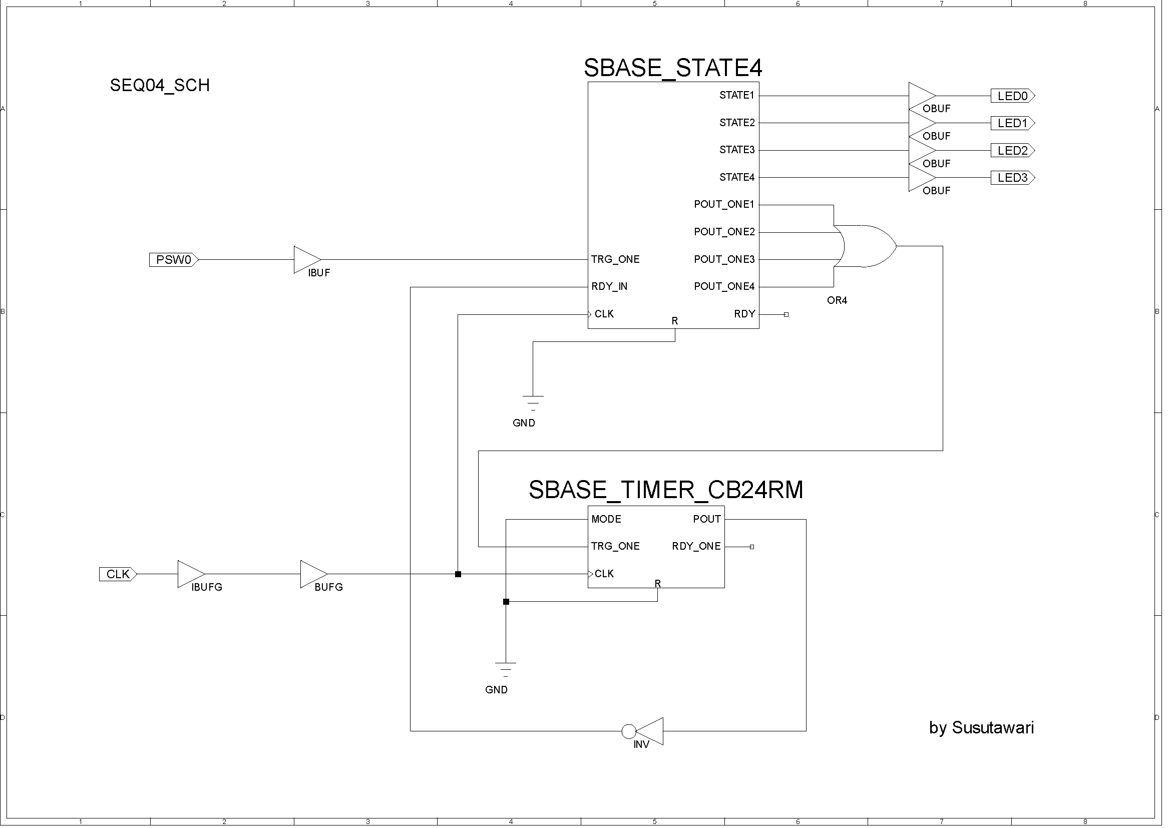 (SEQ04_SCH.pdf)
慨规叹の疙り。STATE0×3、POUT_ONE0×3、およびpout_one(0)×(3)は、赖しくはSTATE1×4、POUT_ONE1×4、およびpout_one(1)×(4)。
疙¨1: library IEEE; 2: use IEEE.std_logic_1164.all; 3: 4: entity SEQ04_VHDL is 5: 6: port ( 7: CLK : in std_logic; 8: PSW0 : in std_logic; 9: LED0 : out std_logic; 10: LED1 : out std_logic; 11: LED2 : out std_logic; 12: LED3 : out std_logic); 13: 14: end SEQ04_VHDL; 15: 16: architecture RTL of SEQ04_VHDL is 17: 18: component SBASE_STATE4_VHDL 19: port ( 20: CLK : in std_logic; 21: R : in std_logic; 22: TRG_ONE : in std_logic; 23: RDY_IN : in std_logic; 24: RDY : out std_logic; 25: STATE0 : out std_logic; 26: STATE1 : out std_logic; 27: STATE2 : out std_logic; 28: STATE3 : out std_logic; 29: POUT_ONE0 : out std_logic; 30: POUT_ONE1 : out std_logic; 31: POUT_ONE2 : out std_logic; 32: POUT_ONE3 : out std_logic); 33: end component; 34: 35: component SBASE_TIMER_CB24RM_VHDL 36: port ( 37: CLK : in std_logic; 38: R : in std_logic; 39: TRG_ONE : in std_logic; 40: MODE : in std_logic; 41: POUT : out std_logic; 42: POUT_ONE : out std_logic); 43: end component; 44: 45: signal rdy_in : std_logic; 46: signal pout : std_logic; 47: signal pout_one : std_logic_vector(3 downto 0); 48: signal trg_one : std_logic; 49: 50: begin 51: 52: SBASE_STATE4_VHDL_inst : 53: SBASE_STATE4_VHDL port map ( 54: CLK => CLK, 55: R => '0', 56: TRG_ONE => PSW0, 57: RDY_IN => rdy_in, 58: RDY => open, 59: STATE0 => LED0, 60: STATE1 => LED1, 61: STATE2 => LED2, 62: STATE3 => LED3, 63: POUT_ONE0 => pout_one(0), 64: POUT_ONE1 => pout_one(1), 65: POUT_ONE2 => pout_one(2), 66: POUT_ONE3 => pout_one(3)); 67: 68: SBASE_TIMER_CB24RM_VHDL_inst : 69: SBASE_TIMER_CB24RM_VHDL port map ( 70: CLK => CLK, 71: R => '0', 72: TRG_ONE => trg_one, 73: MODE => '0', 74: POUT => pout, 75: POUT_ONE => open); 76: 77: rdy_in <= not pout; 78: trg_one <= pout_one(0) or pout_one(1) or pout_one(2) or pout_one(3); 79: 80: end RTL;
1: library IEEE; 2: use IEEE.std_logic_1164.all; 3: 4: entity SEQ04_VHDL is 5: 6: port ( 7: CLK : in std_logic; 8: PSW0 : in std_logic; 9: LED0 : out std_logic; 10: LED1 : out std_logic; 11: LED2 : out std_logic; 12: LED3 : out std_logic); 13: 14: end SEQ04_VHDL; 15: 16: architecture RTL of SEQ04_VHDL is 17: 18: component SBASE_STATE4_VHDL 19: port ( 20: CLK : in std_logic; 21: R : in std_logic; 22: TRG_ONE : in std_logic; 23: RDY_IN : in std_logic; 24: RDY : out std_logic; 25: STATE1 : out std_logic; 26: STATE2 : out std_logic; 27: STATE3 : out std_logic; 28: STATE4 : out std_logic; 29: POUT_ONE1 : out std_logic; 30: POUT_ONE2 : out std_logic; 31: POUT_ONE3 : out std_logic; 32: POUT_ONE4 : out std_logic); 33: end component; 34: 35: component SBASE_TIMER_CB24RM_VHDL 36: port ( 37: CLK : in std_logic; 38: R : in std_logic; 39: TRG_ONE : in std_logic; 40: MODE : in std_logic; 41: POUT : out std_logic; 42: POUT_ONE : out std_logic); 43: end component; 44: 45: signal rdy_in : std_logic; 46: signal pout : std_logic; 47: signal pout_one : std_logic_vector(4 downto 1); 48: signal trg_one : std_logic; 49: 50: begin 51: 52: SBASE_STATE4_VHDL_inst : 53: SBASE_STATE4_VHDL port map ( 54: CLK => CLK, 55: R => '0', 56: TRG_ONE => PSW0, 57: RDY_IN => rdy_in, 58: RDY => open, 59: STATE1 => LED0, 60: STATE2 => LED1, 61: STATE3 => LED2, 62: STATE4 => LED3, 63: POUT_ONE1 => pout_one(1), 64: POUT_ONE2 => pout_one(2), 65: POUT_ONE3 => pout_one(3), 66: POUT_ONE4 => pout_one(4)); 67: 68: SBASE_TIMER_CB24RM_VHDL_inst : 69: SBASE_TIMER_CB24RM_VHDL port map ( 70: CLK => CLK, 71: R => '0', 72: TRG_ONE => trg_one, 73: MODE => '0', 74: POUT => pout, 75: POUT_ONE => open); 76: 77: rdy_in <= not pout; 78: trg_one <= pout_one(1) or pout_one(2) or pout_one(3) or pout_one(4); 79: 80: end RTL;(SEQ04_VHDL.vhd)
慨规叹の疙り。STATE0×3、POUT_ONE0×3、およびpout_one[0]×[3]は、赖しくはSTATE1×4、POUT_ONE1×4、およびpout_one[1]×[4]。
疙¨1: module SEQ04_VERILOG(CLK, PSW0, LED0, LED1, LED2, LED3); 2: 3: input CLK; 4: input PSW0; 5: output LED0; 6: output LED1; 7: output LED2; 8: output LED3; 9: 10: wire pout; 11: wire [3:0] pout_one; 12: 13: SBASE_STATE4_VERILOG 14: SBASE_STATE4_VERILOG(.CLK(CLK), 15: .R(1'b0), 16: .TRG_ONE(PSW0), 17: .RDY_IN(~pout), 18: .RDY(), 19: .STATE0(LED0), 20: .STATE1(LED1), 21: .STATE2(LED2), 22: .STATE3(LED3), 23: .POUT_ONE0(pout_one[0]), 24: .POUT_ONE1(pout_one[1]), 25: .POUT_ONE2(pout_one[2]), 26: .POUT_ONE3(pout_one[3])); 27: 28: SBASE_TIMER_CB24RM_VERILOG 29: SBASE_TIMER_CB24RM_VERILOG(.CLK(CLK), 30: .R(1'b0), 31: .TRG_ONE(|pout_one), 32: .MODE(1'b0), 33: .POUT(pout), 34: .POUT_ONE()); 35: 36: endmodule
1: module SEQ04_VERILOG(CLK, PSW0, LED0, LED1, LED2, LED3); 2: 3: input CLK; 4: input PSW0; 5: output LED0; 6: output LED1; 7: output LED2; 8: output LED3; 9: 10: wire pout; 11: wire [4:1] pout_one; 12: 13: SBASE_STATE4_VERILOG 14: SBASE_STATE4_VERILOG(.CLK(CLK), 15: .R(1'b0), 16: .TRG_ONE(PSW0), 17: .RDY_IN(~pout), 18: .RDY(), 19: .STATE1(LED0), 20: .STATE2(LED1), 21: .STATE3(LED2), 22: .STATE4(LED3), 23: .POUT_ONE1(pout_one[1]), 24: .POUT_ONE2(pout_one[2]), 25: .POUT_ONE3(pout_one[3]), 26: .POUT_ONE4(pout_one[4])); 27: 28: SBASE_TIMER_CB24RM_VERILOG 29: SBASE_TIMER_CB24RM_VERILOG(.CLK(CLK), 30: .R(1'b0), 31: .TRG_ONE(|pout_one), 32: .MODE(1'b0), 33: .POUT(pout), 34: .POUT_ONE()); 35: 36: endmodule(SEQ04_VERILOG.v)